| Home |
| What's New |
| Videos |
| Pictures |
| Donations |
| Webcams |
| Sponsors |
| About us |
| Contact |
| Archives |
| How we do it |
| Quick facts |
| Awards |
| Comments |
| Credits |
| FAQs |
| Lost/Found |

Buffer Boards
|
Setup Status Power Distribution Computer Control Buffer Boards Channel Boxes Snowball Fight Driveway Arches |
Donation Box Grass Grid Roof Grid LED Mega Tree Trees Leaping Arches |
To prevent the computer from higher voltages, required by the lights, buffer boards were created. These boards receive digital outputs from the computer I/O card and isolate the computer voltage entirely from the main supply voltage. The I/O cards can source a max of 2.5mA for each channel, but to power our channel boxes, we need about 30mA for each channel. The buffer boards incorporate opto-isolators and buffers that allow us to supply this higher current to the channel boxes. Details follow:
|
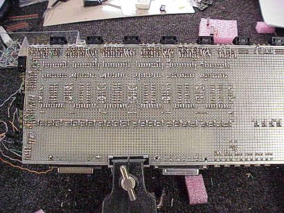
This is the first board we created in 2000. It was basically a test board that, later, led to the design/construction of printed circuit boards. |
| It housed 48 Channels and housed the following components:
1. Current limiting resistor (x6) The board had no traces, so each circuit had to be made by using 24 awg. copper wire. This was a daunting task that consumed many hours of our free time. |
|
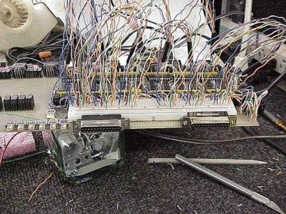 |
The purpose of the buffer chip was to draw as little current from the computer, but provide a larger sourcing output for the opto-isolators. A current limiting resistor was used to limit the buffer current draw to a mere 1.5 ma. The buffers provide 25 ma of output power to the opto-isolators, but the isolators needed to be limited to only 15 ma. This is where the second resistor came into the picture. |
 |
From the isolators, the signal flows to the LED's, this allows us to visually recognize which circuits may/may not be operating. The signal continues to a jumper board which provides us with the flexibility of switching channels easily. From the jumper board, the signal then flows to RJ-45 connectors. This is where we plug in our external switching circuitry, the channel boxes, that house the Triac circuits. |
 |
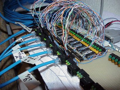
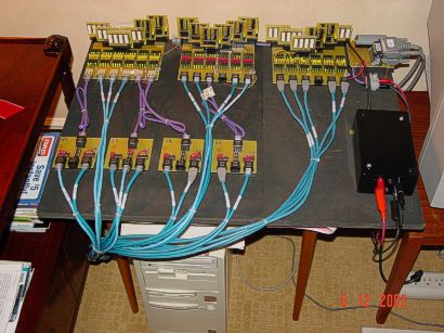
These are the 2nd generation buffer boards. In this round, we couldn't bare the thought of soldering all those wires to create more channels. Thus, we invested/researched in the design and fabrication of Printed Circuit Boards. This method took us a few tries to perfect, but was well worth the effort in the end. The PC boards were designed, fabricated, and assembled by us. Each of the above boards are 48 channels, totaling 96. |
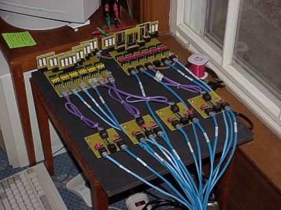 |
To save space, we decided to build a main board, and have the sub channel boards mount perpendicular to the main board. This would allow us to expand on more than one axis which allows us to expand vertically and horizontally. |
The main board consists of an IDC50 pin connector which accepts the inputs from the computer digital I/O card. The signal is directed to the IDC20 pin connectors, to which the sub channel boards are plugged. The sub channel boards are comprised of resistors, opto-couplers, and LED's. These boards provide the necessary power required for the switching circuit. The signal is sent back through the IDC20 pin connector to the main board, then to the 1st set of LED's. This 1st set shows us which output channel is operating, while the 2nd set shows us which box channel is operating. |
|
 |
The second set of small boards in this picture allow us to combine multiple RJ45 connectors that may carrying less than 8 channels, with other RJ45 connectors that are carrying less than 8 channels. This way we are able to utilize all of the channels and eliminate gapping in our channel selection. |